
23 October 2026, 14:38
Loading...
Potential for using photovoltaic resources in Czechia and worldwide (part 1)
Vladimír Wagner
15 January 2018, 19:17
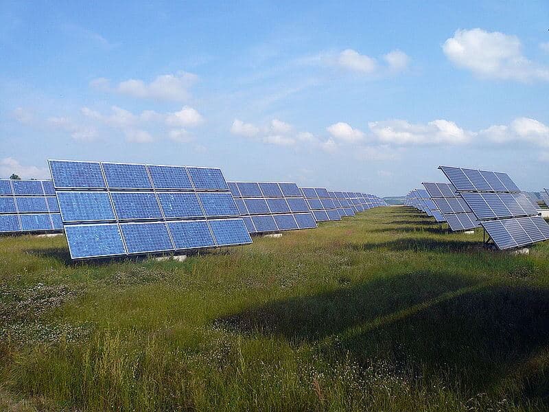
The installed capacity of photovoltaic power plants is currently growing faster than that of any other electricity source. As the price of solar panels falls and electricity storage options expand, expectations for their share in the energy mix are also rising. However, current energy storage technologies still severely limit the potential uses of photovoltaics. The Czech state energy policy also envisages the use of this source. It is therefore worthwhile to examine its characteristics in greater detail.
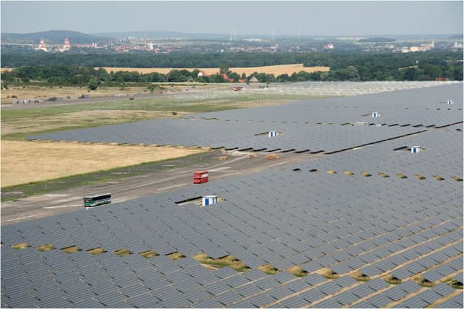
Sunlight is the source of energy for the vast majority of processes on the Earth's surface, including almost all forms of life. The expansion of civilisation in recent centuries has been enabled by the use of fossil fuels, i.e. solar energy stored in fuels. Humanity consumes average power of around 18 TW, only a small fraction of the approximately 174 000 TW of power that the Sun sends to Earth.
By comparison, photosynthetic activity on Earth corresponds to average power of around 130 TW, only several times more than human civilisation consumes. It should be added that humans use around one-quarter of the photosynthesis taking place on Earth for their own purposes, which is many times more than the capacity of all solar power plants installed to date, which reached approximately 300 GWp at the beginning of 2017 (the unit Wp, or watt peak, denotes the maximum output of a photovoltaic cell or system under full illumination and optimal conditions).
It is also interesting that modern photovoltaic cells achieve substantially higher energy conversion efficiency than photosynthesis. The research that led to today's highly efficient solar cells has a story involving surprising inspirations and dramatic twists, and it is worth telling.
History of using solar energy through photovoltaic cells
The discovery of photovoltaic conversion dates back to 1839, when, at the age of 19, Alexandre-Edmond Becquerel observed electrical effects in an electrolytic cell caused by incident light in his father's laboratory. The phenomenon soon found practical application in photographic exposure meters, but the energy conversion efficiency of the cells of the time, based on amorphous selenium or cuprous oxide, was too low for practical use. Even in 1931, when Thomas Alva Edison said in an interview with Henry Ford that he would invest in solar energy, efficiency had not exceeded 1 %.
A breakthrough came in 1953 at Bell Laboratories, the research centre of telephone company AT&T (American Telephone and Telegraph Company). Telephone lines needed power sources for repeater amplifiers, and the batteries used were unreliable. The company therefore asked Daryl Chapin to investigate other possible energy sources (the brief mentioned wind turbines, thermoelectric sources and steam generators). Chapin proposed using photovoltaic cells, but existing selenium cells delivered a maximum of 5 W per square metre. Bell Laboratories was also the place where the first semiconductor components were developed (including the transistor in 1947). Chapin's friends Gerald Pearson and Calvin Fuller were working on methods of silicon doping and managed to create a planar pn junction in silicon wafers. The aim was to achieve 6% efficiency, which was indeed accomplished using silicon wafers doped with arsenic and with a phosphorus-doped surface layer. The resulting cell was approximately the size of a conventional razor blade, delivered a voltage above 0.5 V and power of ~60 W/m2.
The discovery was announced at a press conference on 25 April 1954, and the press described it as the “beginning of a new era in harnessing the Sun's unlimited energy” (Times) and speculated that “one day solar cells may produce more energy than sources based on coal, oil or nuclear power” (New York Times). Each of the three authors then received a symbolic reward of $1 for transferring the patent rights to their employer.
At that time, less than 1 Wp of silicon cells had been produced, but despite their high price, production of prototypes of the first solar panels began. However, tests of practical use in Americus, Georgia, were disappointing: the panels worked, but suffered from shading problems and, above all, at prices of hundreds of dollars per Wp they were simply too expensive. For a time, it appeared that photovoltaic cells would remain a curiosity. Indeed, Chapin, Fuller and Pearson were already working on another topic at the time, namely power semiconductor components.
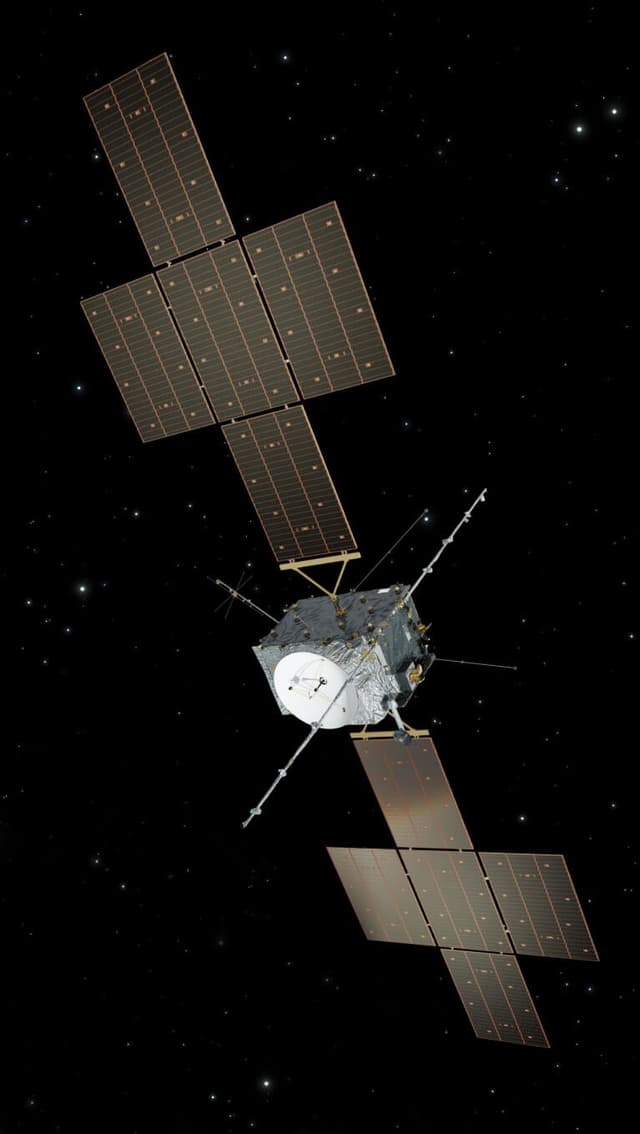
A dramatic turn in the history of photovoltaics came at the turn of 1957 and 1958, after the Soviet Union launched Sputnik, the first artificial Earth satellite, into orbit on 4 October 1957. At a time of the nuclear arms race, the news was an unexpected shock to people in the United States. The US responded by accelerating its space programme (as well as strengthening the budget of the NSF grant agency and teaching of science and engineering subjects in schools). Half a year later, Vanguard 1 was launched into orbit (around 50 times lighter than Sputnik). Vanguard 1 was fitted with six small solar panels that powered a 5 mW radio transmitter. It operated until 1964, substantially longer than the preceding Sputnik 1 and 2 and Explorer 1 satellites powered by chemical batteries. Powering space technology with solar panels became standard, and photovoltaics thus gained its first commercial application, where the high cost of cells was not an obstacle. A detailed popular article on the history and future of photovoltaic cells in space was published here.
Properties of modern photovoltaic cells
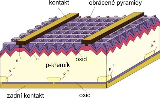
The photovoltaic conversion efficiency of silicon solar cells increased more than fourfold between 1957 and the end of the century, reaching 25 % in 1998. This record was achieved by the laboratory of Professor Martin Green at the University of New South Wales in Sydney using a special laboratory cell with an area of 4 cm2, produced using a range of measures to improve efficiency. The upper surface of the cell is structured into microscopic pyramids covered by a double anti-reflective layer. The pyramids improve light capture and result in a high density of photogenerated current. Dopants on the rear side of the cell were concentrated in locally diffused point contacts. This structure also entered production at Chinese company Suntech.
The efficiency record for silicon wafer cells was not surpassed until 16 years later by industrial laboratories using cells with an area employed in actual production. The record was matched by SunPower and then exceeded several times by Japanese heterojunction cells developed by Sanyo (now Panasonic). The current record of 26.6 % is held by Kaneka. However, scope for further increases in efficiency is already very limited, as current values are approaching the physical limit known as the Shockley-Queisser limit, which is 29.4 % for silicon.
To understand the Shockley-Queisser limit, it is necessary to explain the basic processes that take place in semiconductor cells during photovoltaic conversion. Each photon of sunlight absorbed in a semiconductor generates an electron in the conduction band and leaves a corresponding hole in the valence band, which behaves as a positive charge. Both the electron and the hole thermalise very rapidly (i.e. reduce their potential energy to the edges of the respective bands). Regardless of its original energy, the maximum usable energy from each photon is therefore equal to the band gap, i.e. the difference between the conduction-band and valence-band edges (1.1 eV for silicon).
It also logically follows that photons with energy lower than the band gap cannot be absorbed and therefore utilised. A large part of infrared light thus remains entirely unused. Further losses occur at contacts and also result from the unavoidable radiative recombination of electrons and holes.
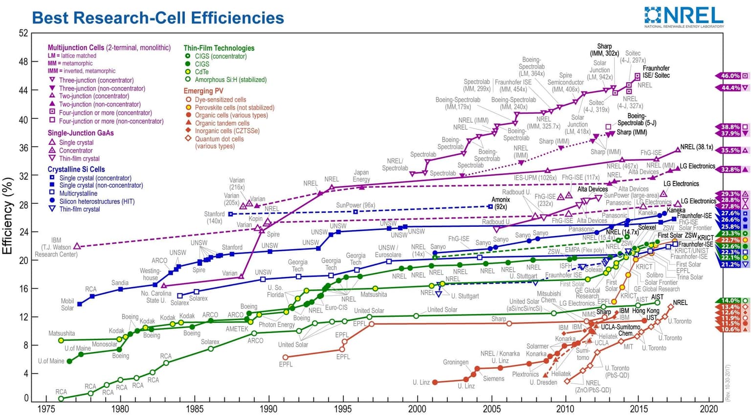
Understanding the Shockley-Queisser limit also points the way to achieving higher efficiency. The National Renewable Energy Laboratory in Golden, Colorado, maintains an overview of record cells, and the values are published in a regularly updated chart. At first sight, it is striking that the highest efficiencies reach substantially higher values than those for silicon, up to 46 %. A closer look at the chart shows that there are several routes to exceeding silicon efficiency. A different semiconductor with a more suitable band gap can be selected and, indeed, for GaAs, for example, achieved efficiency approaches 29 % against a limiting efficiency of 33.5 %. Photovoltaic conversion efficiency also rises with the concentration of sunlight (usually stated as the number of suns, x). For silicon, efficiency of 27.6 % has thus been achieved at 92x concentration, and for GaAs 29.1 % at 117x. A substantially greater increase in efficiency can be achieved using tandem cells with multiple band gaps: light first passes through a cell with a larger band gap, which makes it possible to use a larger share of the energy of absorbed photons. Photons with energy lower than the band gap of the first cell then pass to another cell with a smaller band gap. The cells are connected in series, so their voltages add up. For a tandem cell to work well as a whole, the photocurrents generated in the individual cells must be matched. The same principle can be applied repeatedly, and the record efficiency of 46 % was achieved using a quadruple GaInP/GaAs; GaInAsP/GaInAs tandem and 508x light concentration.
However, these record cells are not suitable for ordinary use because they require special panel designs with precise tracking of the Sun throughout the day, are unsuitable for use in situations where sunlight is scattered by, for example, aerosols in the atmosphere, and above all, their production requires extraordinary costs.
From another perspective, cells located in the lower part of the aforementioned chart may be more interesting. Here we find a diverse group of cells typically produced as thin layers of semiconductors or organic dyes in a mixture with an inorganic matrix, such as TiO2. Their main advantage is above all the possibility of producing them at far lower cost and with lower energy requirements for their manufacture. This determines the time in which the corresponding photovoltaic panels achieve energy payback. Under typical Central European conditions, this is around two years for panels using silicon wafers, but can be less than one year for thin-film panels. Given an expected panel lifetime of around 25 years, this results in relatively high energy returns, at around 10 to 20 times. In this comparison, thin-film panels perform significantly better, because silicon wafers are the most energy-intensive component of conventional panels. Producing silicon wafers with the required purity level is around ten times more demanding in terms of energy expended than all other panel components. Meanwhile, conventional thin-film panels use only a silicon layer around 1 micrometre thick, compared with a typical silicon wafer thickness of 100 to 250 μm.
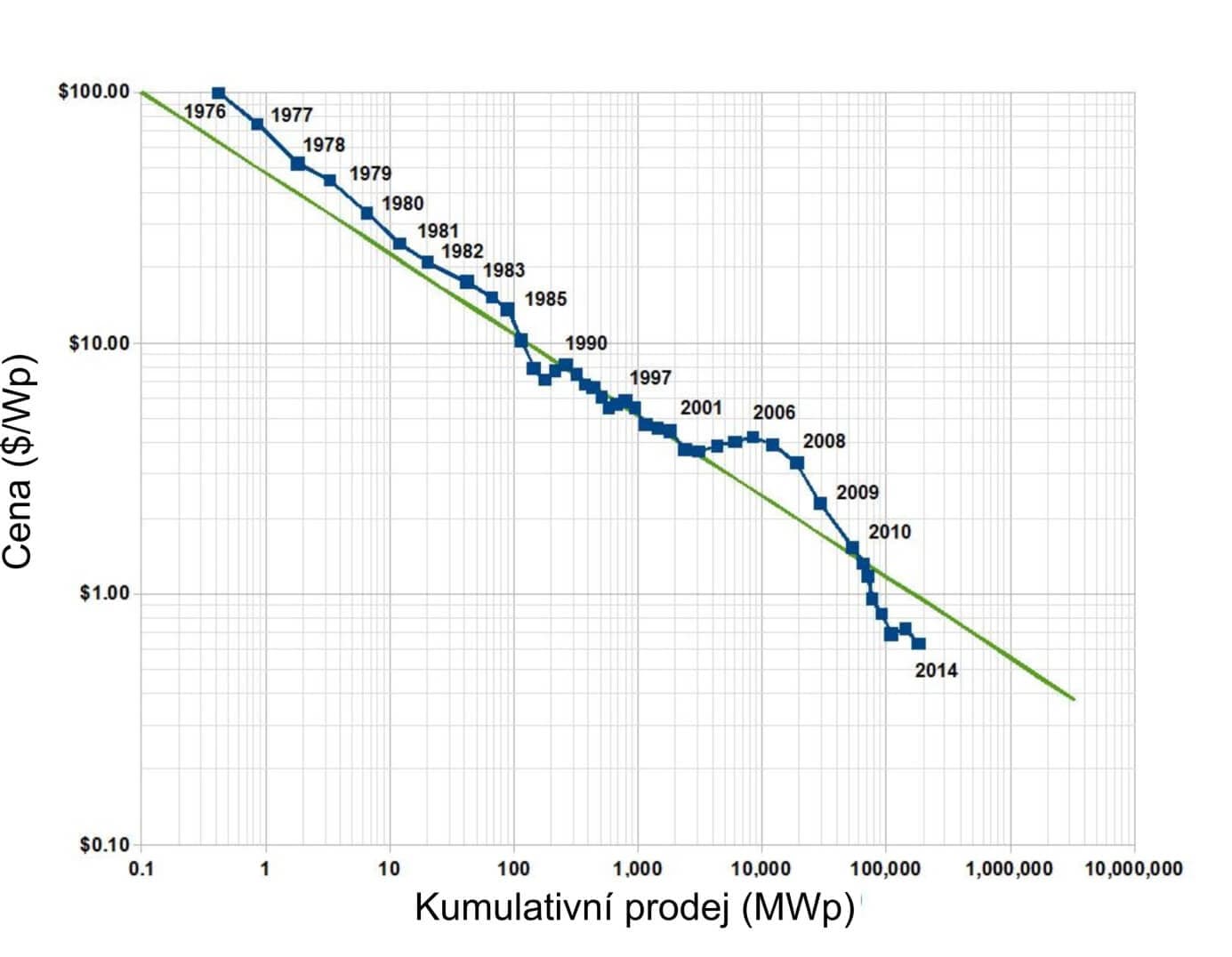
Despite this advantage, the vast majority of photovoltaic panels are currently based on silicon wafers. The reason is, of course, economic. Mass production of solar cells has led to a marked price decline in recent years, known as Swanson's law of solar energy. Like Moore's law for computer development, Swanson's law is actually an empirical observation that doubling photovoltaic module production reduces the price by 20 %. The law is named after Richard Swanson, founder of SunPower, and describes the photovoltaic learning curve.
The learning curve has been exploited primarily by manufacturers of silicon wafer-based panels, and as a result production costs for these panels are currently around $0.5/Wp or less (although it should be mentioned that, especially in recent years, part of the price reduction has been achieved by shifting a large part of production to low-cost countries, particularly China, and the recent closure of some polluting facilities in China is pushing prices higher).
The production cost of $0.5/Wp is important in several respects. Until recently, panel costs were the main reason photovoltaic electricity could not compete directly with conventional sources economically. However, this has changed in the past few years, and so-called grid parity has been reached in a number of countries, meaning that the price of photovoltaic electricity, including all costs over the power plant's life cycle, is equal to the price at which electricity could be purchased from the grid.
A second consequence is that the price of panels is now only a smaller part of photovoltaic system costs, with costs for the so-called balance of system — mounting structures, inverters, grid connection and operation — predominating overall. These costs are mostly directly proportional to system area, which favours higher-efficiency panels. Conversely, despite their higher energy return, thin-film panels have gradually become uncompetitive due to their lower efficiency, and their production is declining both relatively and absolutely. This results in a technology lock-in effect, in which silicon wafer panels dominate the market and use rapid growth to achieve further cost reductions.
How to achieve higher efficiency – perovskites
For other cells to have a chance of gaining ground, a way would have to emerge to achieve high efficiency for them as well. In this respect, another surprising turn came just a few years ago with the emergence of organic-inorganic perovskite solar cells with the chemical formula CH3NH3PbX3 , where X is Cl, Br or I. The first experiments were carried out by Professor Miyazaki's group in 2009 and achieved efficiency of 3.8 %. Since then, the achieved efficiency values have risen extraordinarily rapidly. By optimising cell production and structure, Professor Seok's group achieved the current record efficiency of 22.7 %. This value is all the more remarkable when one considers that these are active layers only 200–300 nm thick, prepared from solutions at ordinary temperatures of up to 100° C. Perovskites could thus become the basis for inexpensive and simple production of highly efficient solar cells.
On the other hand, it should be stressed that perovskite solar cells also have drawbacks. The first fundamental problem is interaction with airborne moisture, which causes chemical decomposition of the perovskite structure, usually gradually reducing photovoltaic conversion efficiency over a timescale of months. The second problem is the content of the heavy metal lead, which may be potentially hazardous despite the relatively small quantities used.
It is therefore clear that the story of seeking ways to use the Sun as a renewable source of electricity will continue with further chapters.
The article will continue in part two…
Article authors: Vladimír Wagner, Antonín Fejfar, Martin Ledinský
Note
This article is the third in a series examining the potential of individual energy sources in Czechia, intended to initiate discussion about the future development of the Czech electricity sector, its challenges and opportunities. In particular, several years have already passed since the last update of the energy policy, while in reality not much has been done in the energy sector. At the same time, a number of risks are emerging, so it is very important to gain an overview of energy developments and conditions both globally and in Czechia. The first part, devoted to wind energy, is available here (part 1) and here (part 2). The second part, devoted to nuclear sources, is available here (part 1) and here (part 2).
The article was originally published on OSEL.CZ.
Studies examining the potential of photovoltaics in Czechia:
J. Jakubes and V. Járka: Study “Potential of solar energy in the Czech Republic”, ENACO for the Czech Photovoltaic Industry Association
Part of the text is based on the article:
A. Fejfar, M. Ledinský, Photovoltaic use of energy from sunlight, Czechoslovak Journal of Physics. 65 (2015) 384–388
Recommended sources:
Translation disclaimer
This article is a machine translation of the Czech original and has not yet been fully reviewed. In case of any doubt, please refer to the Czech version.
Sdílejte článek prostřednictvím:
You might also like
23 October 2026, 11:01

23 October 2026, 06:34